As integrated circuit (IC) technology advances and circuits become more powerful and compact, identifying and preventing potential causes of circuit failure is essential. One particularly critical factor contributing to circuit failure is electromigration within metallic interconnects, stemming from the accumulation of vacancies. This blog post will review the governing equations that describe electromigration and demonstrate how to model this phenomenon using the COMSOL Multiphysics® software.
The Effects of Electromigration
Devices we use daily, such as computers or smartphones, rely on ICs. These devices contain CPUs, GPUs, or RAM chips, which can contain millions or billions of semiconductor components to perform various calculations when processing data. These calculations can only be performed if signals can be reliably transferred between the semiconductor components. This task is accomplished via interconnects — conductive pathways that allow currents to flow between components.
Over time, due to extended use of the IC, an interconnect can experience damage and may even completely fail due to electromigration. Although electromigration can occur in a metal of any size, it is more of a concern in small-scale components, which can contain features on the order of nanometers. For perspective, there are a few dozen atoms in a cubic nanometer of copper, a common material used for interconnects.
Electromigration occurs when vacancies within a crystal lattice move and accumulate to form macroscopic voids (regions with no atoms) or hillocks (regions where atoms accumulate). This can lead to an increase in electric resistance, overheating, material degradation, and an overall weakening of the structure. Macroscopic void growth and hillock formation can result in the failure of the interconnect due to electrical shorting or an open circuit.
Image of a failure location caused by electromigration. Image in the public domain, via Wikimedia Commons.
A vacancy is a site within a crystalline structure where an atom is missing. In a perfect crystal lattice, there would be no vacancies, but in reality, any crystal will contain some number of vacancies. Vacancies may form during the solidification of a metal (or alloy) or arise spontaneously due to random atomic vibrations. Random atomic motion occurs at any temperature above absolute zero, and at a particular temperature, every lattice will have some equilibrium concentration of vacancies distributed throughout it.
Although we refer to the migration or movement of the vacancies, physically, the vacancies themselves are not moving, but rather the atoms move by jumping into neighboring vacancies, which is known as “substitutional diffusion”. The vacancy appears to migrate in the direction opposite to the motion of the atoms. At the nanoscale, there are many vacancy jumps taking place throughout the material, even in the absence of external fields. At the macroscale, there is no overall vacancy movement, since the nanoscale motion is isotropic at equilibrium. However, in the presence of external driving forces, there will be atomic motion and therefore vacancy motion in a certain direction.
What Aspects Contribute to Vacancy Flux
One of the main contributors to vacancy motion in an interconnect is the electric current flowing through it. When a potential difference is applied across the interconnect, the electrons experience a force in the direction of the electric field resulting in a net motion of electrons. As the electrons flow through the conductor, some collide and transfer energy and momentum to the atoms. This momentum transfer causes some of the atoms to gain enough energy to jump to a neighboring vacancy. The flux of vacancies generated by this effect is given by:
1
\mathbfJ_E =\fracD_vkT c_v \vecE
where c_v is the vacancy concentration, D_v is the vacancy diffusivity, z^* is the effective charge number, e is the elementary charge, \vecE is the electric field, k is Boltzmann’s constant, and T is the temperature.
Since the structural properties and the electrical conductivity are usually a function of temperature, it is necessary to accurately solve for the temperature distribution in the interconnect.
In describing the vacancy flux due to an electric field, it was mentioned that the electrons flow through the conductor and lose energy due to collisions with atoms. It is therefore also important to account for the Joule heating as a result of this energy transfer. As interconnects are quite small, the current density can be high, and the Joule heating is not negligible.
The thermal gradient that arises due to Joule heating and heat transfer with the surroundings also influences the movement of atoms and vacancies. The additional vacancy flux given by the temperature gradient reads:
2
\mathbfJ_T = -\fracD_vQ^*kT^2 c_v \nabla T
where Q* is the heat of transport.
Another contribution to vacancy motion is due to the diffusion of vacancies from high to low concentrations. This flux is proportional to the gradient of the vacancy concentration:
3
\mathbfJ_D = -D_v \nabla c_v
Note that the diffusion coefficient may be dependent on the temperature or the stress within the material. In addition, the lattice microstructure has a large influence on the diffusion coefficient. Atoms (and vacancies) encounter significantly less resistance to motion at grain boundaries; thus, if the interconnect is manufactured in a way that it contains many small grains, there would be more grain boundaries to serve as pathways for diffusion, and the overall effective diffusion coefficient will be higher. The orientation of the grains relative to the current flow also significantly influences the diffusivity.
Due to thermal expansion and vacancy accumulation, the material may deform causing damage which can result in interconnect failure. Therefore, resolving the stress distribution within the material is needed.
Atoms tend to migrate from high-stress to low-stress areas; thus, vacancies migrate in the opposite direction. This flux generally opposes the flux due to the electric field, and is given by:
4
\mathbfJ_\sigma = -\fracD_vf \OmegakT c_v \nabla \sigma
where f is a material-specific vacancy relaxation factor, \Omega is the atomic volume, and \sigma is the hydrostatic stress.
Now that all of the contributions to the vacancy motion have been introduced, the total vacancy flux is given by the sum:
5
\mathbfJ_v = \mathbfJ_D + \mathbfJ_E + \mathbfJ_\sigma + \mathbfJ_T
A standard transport equation is then solved considering the overall flux,
6
\frac\partial c_v\partial t +\nabla \cdot \mathbfJ_v = G
where G is a source/sink term due to the generation or annihilation of vacancies within the domain.
Another effect to consider is the shrinkage of the lattice in regions where vacancy accumulation occurs and the swelling in regions where the vacancy concentration decreases. This behavior is described by the volumetric strain rate due to the divergence of the vacancy flux and vacancy generation:
7
\frac\partial \epsilon_vol\partial t = \Omega \left( f \nabla \cdot\mathbfJ_v + (1 – f) G \right)
Modeling Electromigration
To model electromigration, we can use COMSOL Multiphysics® to solve multiple different physics simultaneously, including electric currents, solid mechanics, heat transfer, and, of course, the transport of the vacancies themselves.
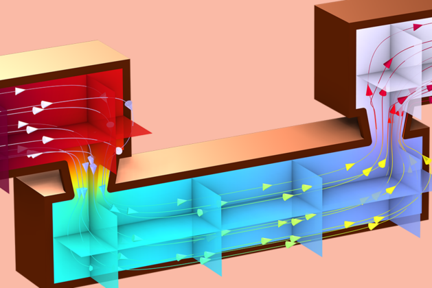
Let’s first take a look at what an interconnect may look like. The image below shows an example geometry of a single interconnect. Materials such as aluminum or copper may be used as the conductive material. Depending on the specific design and materials chosen, there may also be a liner or barrier surrounding the primary interconnect material. These layers are added for a few reasons, such as to prevent the diffusion of atoms into the surrounding dielectric or to improve adhesion between the interconnect and a dielectric material.

A typical interconnect geometry.
The Electric Currents interface can be used to solve for the electric potential throughout the domain based on the boundary conditions and material properties we have defined. Regardless of the geometric details, there will be a boundary which acts as a ground (V=0), and another boundary where a known potential, current, current density, or power is specified.
The Solid Mechanics and Heat Transfer in Solids interfaces are used to consider the structural and thermal response of the interconnect. The material is assumed to be linear elastic, and in this example, material nonlinearities are not considered.
To define appropriate boundary conditions in the Heat Transfer in Solids interface, the surrounding thermal environment must be considered. For example, the entire chip may be cooled via forced or natural convection. In this model, a convective heat flux condition is applied on the external boundaries of the liner, while the ends of the interconnect have a fixed temperature.
As discussed, the primary heat source within the interconnect is due to the Joule heating effect, which can be readily considered with the Electromagnetic Heating multiphysics coupling. Additionally, thermal expansion is accounted for with the Thermal Expansion multiphysics coupling.
There are numerous tutorials available on modeling Joule heating and thermal expansion with COMSOL®. For example, the Getting Started with Electro-Thermal Mechanical Modeling series introduces the workflow for setting up these problems.
The Transport in Solids interface can be used to set up the governing equations to model the vacancy transport. This interface solves a transport equation for the concentration of the variable of interest, which in this case is the vacancy concentration.
By default, the transport equation considers the diffusive flux due to concentration gradients. However, to model the total flux due to electromigration, additional flux contributions can be added. The Transport in Solids interface makes it easy to incorporate these additional contributions into our governing equations using the External Flux feature, as shown in the following image.
The External Flux feature can incorporate any additional fluxes to the transport equation.
We can see that the flux contributions from the electric field, stress, and temperature gradients have been added to this model. The corresponding flux variables are defined in the Variables section with the expressions outlined above.
Variables to include strain rate, temperature flux, and vacancy source/sink terms.
To consider the volumetric swelling due to vacancy accumulation, we can add an External Strain subnode to the Linear Elastic Material node. This feature allows the specification of any inelastic strain contribution. Thermal expansion and creep are typical examples of inelastic strains that can also be considered.
Results
It is common to solve electromigration models with a transient analysis since usually we are interested in how long it will take to reach a certain critical condition. Of course, if we solve a transient study, the solution will eventually reach a steady state, and the time this takes may also be of interest. We will take a look at a few key results from running a transient study until the solution reaches a steady state.
One key result to look at is the vacancy concentration within the interconnect since this is the main variable we are solving for in the transport equation. The initial vacancy concentration is set equal to a constant equilibrium value throughout the entire domain. As electromigration occurs, the vacancy concentration near the anode decreases, whereas the vacancy concentration at the cathode (where current is applied) increases. This occurs until a steady state condition is reached. The flux caused by the electric field generally points to the opposite direction of the flux due to hydrostatic stress. The vacancies move from the anode to the cathode until other flux contributions (the hydrostatic flux and the diffusive flux) balance the flux due to the electric field.
The plot below shows the normalized vacancy concentration once the transient solution has reached a steady state. Note that the normalized concentration is defined by the vacancy concentration divided by the initial concentration (so at t=0 s, the normalized concentration is equal to one).
The surface plot shows the normalized vacancy concentration at t=4.5e6 s. The streamlines follow the electric field and are colored to show the electric potential.
In addition, it can be useful to take a look at how the vacancy concentration changes with time on the anode and cathode. From the following plot, we can observe that the flux of vacancies at some point reaches a steady state concentration. The time until a critical vacancy concentration is exceeded may also be of interest.
The normalized vacancy concentration at the anode and cathode versus time.
Similarly, the hydrostatic stress, which contributes to the vacancy flux, can be obtained at the anode and cathode boundaries versus time.
The hydrostatic stress at the anode and cathode versus time.
Von Mises stress(MPa) within the aluminum interconnect at t=4.5e6 s.
The von Mises stress may be an indicator of when a macroscopic void nucleates. Keep in mind, however, that stresses at sharp corners may be singular, and you may want to introduce fillets to avoid this phenomenon. More information on singularities in structural mechanics can be found in our “Singularities in Finite Element Models” blog post.
Transport in Solids
When modeling electromigration, the structural response, particularly the stress and strain within the domain, must be considered. As discussed, there is vacancy flux due to the stress gradient. Additionally, we may want to ensure that the stress does not exceed the yield stress anywhere in the domain for example. If deformations and rotations are fairly small, we may assume a geometrically linear analysis.
Further Modeling
Up to this point, we have covered the theory and setup of COMSOL Multiphysics® for the fundamental vacancy transport equation. We have also touched upon relevant physics such as heat transfer, electric currents, and solid mechanics, as these aspects must be considered when modeling electromigration. The model discussed so far is suitable to describe the initial stage of electromigration before failure occurs.
Our model can be used to predict the onset of void nucleation. Although there is no universal agreement on the exact conditions for void nucleation, it has been suggested that void may form once a critical vacancy concentration or stress level is reached. Some researchers also propose that voids may nucleate at grain boundaries or preexisting free surfaces, where the stress level required for void formation is reduced.
Monitoring these criteria can assist in predicting where and when voids may nucleate within the domain or on a boundary. Once nucleation occurs, it may then be of interest to track void motion and growth. While this is more challenging, COMSOL Multiphysics® can handle this as well. You can set up such simulations using interface tracking methods like the level set or phase field methods. A few examples which employ these methods are linked below:
Conclusion
This blog highlights the importance of accurately modeling vacancy transport in predicting interconnect failure. By taking advantage of the multiphysics simulation capabilities of COMSOL Multiphysics®, we can gain insight into electromigration phenomena and more effectively predict the onset of void formation and assess its impact on device performance.
Next Steps
Try out a model similar to the one discussed in this blog post by clicking the button below, which will take you to the Application Gallery:
References
- Orio, R. L. de, et al. “Physically Based Models of Electromigration: From Black’s Equation to Modern TCAD Models.” Microelectronics Reliability, vol. 50, no. 6, Elsevier BV, June 2010, pp. 775—89.
Leave a comment